Pin share or I call it pinmux, it is a common feature of most MCU chips. Normally a pin we can use it as GPIO or some special functions.
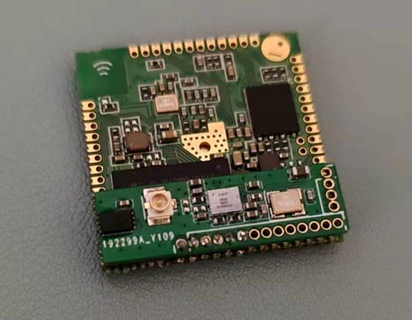
In picture, the orange number is each pins GPIO number. And in the color block, there is its special function.
Here is a table from vocore.io/v2.html, for example, the pin 29 on the chip has three functions, one is used as GPIO, one is system reference clock, final one is SDcard CLK.
Left | Name | Mux | Note |
---|---|---|---|
– | +3.3VO | +3.3V output | max output current 100mA |
30 | TXD0 | GPIO12, UART0 Lite TXD | pull down to GND, Test/Normal mode pin. |
31 | RXD0 | GPIO13, UART0 Lite RXD | 3.3V |
29 | REFCLK | GPIO11, reference clock, SDXC CLK* | |
33 | P0RP | 10/100 PHY Port #0 RXP | |
34 | P0RN | 10/100 PHY Port #0 RXN | |
35 | P0TP | 10/100 PHY Port #0 TXP | |
36 | P0TN | 10/100 PHY Port #0 TXN | |
43 | TXD2 | 10/100 PHY Port #1 TXN, GPIO15, PWM Channel, SPI Slave Clock | |
44 | RXD2 | 10/100 PHY Port #1 TXP, GPIO14, PWM Channel, SPI Slave Chip Select | |
40 | PWM0 | 10/100 PHY Port #1 RXN, GPIO17, UART2 Lite TXD, SPI Slave MOSI | 4.7K pull down to GND |
42 | PWM1 | 10/100 PHY Port #1 RXP, GPIO16, UART2 Lite RXD, SPI Slave MISO | |
45 | P2RP | 10/100 PHY Port #2 RXP, GPIO18, PWM Channel | |
46 | P2RN | 10/100 PHY Port #2 RXN, GPIO19, PWM Channel | |
47 | P2TP | 10/100 PHY Port #2 TXP, GPIO20, PWM Channel | |
48 | P2TN | 10/100 PHY Port #2 TXN, GPIO21, PWM Channel | |
49 | SD WP | GPIO22, 10/100 PHY Port #3 TXP, SDXC WP | |
50 | SD CD | GPIO23, 10/100 PHY Port #3 TXN, SDXC CD |
Top | Name | Mux | Note |
---|---|---|---|
– | GND | Groud | |
28 | SPI CS0 | SPI Master Chip Select 0 | 4.7K pull up to 3.3V |
25 | SPI CLK | SPI Master Clock | 4.7K pull up to 3.3V |
26 | SPI MISO | SPI Master In Slave Out | |
27 | SPI MOSI | SPI Master Out Slave In | 4.7K pull down to GND |
24 | SPI CS1 | SPI Master Chip Select 1 | 4.7K pull down to GND |
21 | I2C SD | GPIO5, I2C Data, SDXC D2* | 4.7K pull up to 3.3V |
20 | I2C CLK | GPIO4, I2C Clock, SDXC D3* | 4.7K pull up to 3.3V |
19 | I2S CLK | GPIO3, I2S Bit Clock, SDXC CMD* | |
18 | I2S WS | GPIO2, I2S L/R Clock, SDXC D0* | |
16 | I2S SDI | GPIO0, I2S Data In, SDXC D1* | |
17 | I2S SDO | GPIO1, I2S Data Out | 4.7K pull down to GND |
Right | Name | Mux | Note |
---|---|---|---|
– | GND | Ground | |
148 | RXD1 | GPIO12, UART1 Lite RXD | |
147 | TXD1 | GPIO13, UART1 Lite TXD | pull up to 3.3V, GPIO/JTAG mode pin |
141 | GPIO41 | GPIO41, JTAG TMS | JTAG needs 10K pull up, R9 -> R6 |
140 | GPIO40 | GPIO40, JTAG Clock | JTAG needs 10K pull up, R9 -> R6 |
139 | GPIO39 | GPIO39, JTAG Reset | JTAG needs 10K pull up, R9 -> R6 |
143 | GPIO43 | GPIO43, JTAG TDO | JTAG needs 10K pull up, R9 -> R6 |
142 | GPIO42 | GPIO42, JTAG TDI | JTAG needs 10K pull up, R9 -> R6 |
138 | RST | Reset, touch GND to reset | |
137 | GPIO38 | GPIO38 | |
136 | GPIO37 | GPIO37 | |
– | +3.3VO | +3.3V output | max output current 100mA |
– | GND | Ground | |
– | +1.8VO | +1.8V output | max output current 100mA |
Bottom | Name | Mux | Note |
---|---|---|---|
– | GND | Ground | |
51 | SD D1 | GPIO24, 10/100 PHY Port #3 RXP, SDXC D1 | |
52 | SD D0 | GPIO25, 10/100 PHY Port #3 RXN, SDXC D0 | |
54 | SD CLK | GPIO26, 10/100 PHY Port #4 RXP, SDXC CLK | |
55 | SD CMD | GPIO27, 10/100 PHY Port #4 RXN, SDXC CMD | |
56 | SD D3 | GPIO28, 10/100 PHY Port #4 TXP, SDXC D3 | |
57 | SD D2 | GPIO29, 10/100 PHY Port #4 TXN, SDXC D2 | |
– | +3.3VO | +3.3V output | max output current 100mA |
61 | USB DP | USB2.0 Data+ | |
62 | USB DM | USB2.0 Data- | |
– | +5.0VI | +5.0V input | min input current 500mA |
– | GND | Ground | |
– | GND | Ground |
Middle | Name | Mux | Note |
---|---|---|---|
133 | PCI CKP | PCI Express External Reference Clock Output+ | |
132 | PCI CKN | PCI Express External Reference Clock Output- | |
130 | PCI RXN | PCI Express Differential Receiver RX- | |
129 | PCI RXP | PCI Express Differential Receiver RX+ | |
– | GND | Ground | |
127 | PCI TXP | PCI Express Differential Transmit TX+ | |
126 | PCI TXN | PCI Express Differential Transmit TX- | |
135 | PCI RST | PCI Express Device Reset |
On VoCore2 Ultimate, ES8388 do not need external clock because we can use VoCore2 system reference clock as its source, in most situation, that will save cost of the BOM.
Set the Pin Function
now, question come, how do we setup every pins function? Sometimes you may want use it as GPIO but sometimes we need to use as clock.
Actually it is same as other MCU(like STM32 and ATMEGA–Arduino) , we have register for every function.
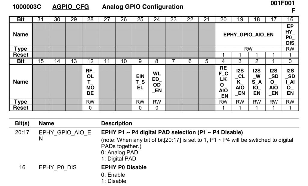
Use this REFCLK pin as example, we can find on MT7628AN datasheet page 117, 2.2 System Control Section, 0x10000060 is that control register.
Its register is 1:0 two bits. (note: on this datasheet, its name is GPIO mode)
We can write 10b to this register, then it will be REFCLK mode.
and after it into REFCLK mode, we can change its frequency, at page 110, 0x1000002c register, bit 11:9 REFCLK0_RATE
And you can use same way to change other pins function 🙂
Also I have a simple tool to do this, please download at vocore.io/v2.html, Directly write to memory/register Section.